With the ever-increasing number of electric vehicles (EVs) in the market, the need to alleviate consumers' range anxiety and charging anxiety has led to the development of bidirectional On-Board Chargers (OBCs). These can not only enable fast charging but also allow EVs to function as distributed energy storage stations, feeding power back into the grid to help balance supply and demand. Utilizing Direct Current Fast Charging (DCFC) to efficiently charge EVs represents a significant trend towards renewable energy transition. Ultra-fast charging stations integrate various components, including auxiliary power supplies, sensors, power management systems, connectivity, and communication devices. They also require flexible manufacturing methods to cater to the evolving charging needs of various EVs, adding complexity to the design of DCFC and ultra-fast charging stations.
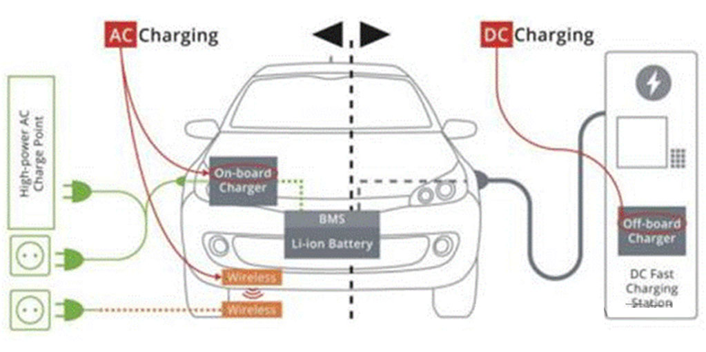
The difference between AC and DC charging lies in their charging mechanisms. For AC charging (left side of Following Picture), the OBC is plugged into a standard AC outlet, converting AC power into the appropriate DC power to charge the battery. In contrast, DC charging (right side of Following Picture) involves the charging station directly supplying power to the battery.
The discrete design of DC charging stations offers maximum flexibility but necessitates a more intricate development process. Modularization, on the other hand, provides numerous performance advantages that are difficult to achieve with discrete designs. For instance, modules integrate multiple power devices within a single compact package, simplifying mechanical assembly, optimizing thermal management, enhancing reliability, and mitigating voltage spikes and high-frequency electromagnetic interference (EMI).
System Components of DC Charging Stations
(1) Entire System Components
(2) System Subcomponents
(3) Functional Block Diagram
(4) Charging Station Subsystems
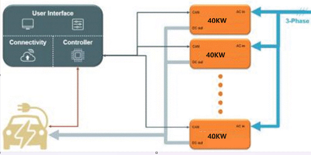
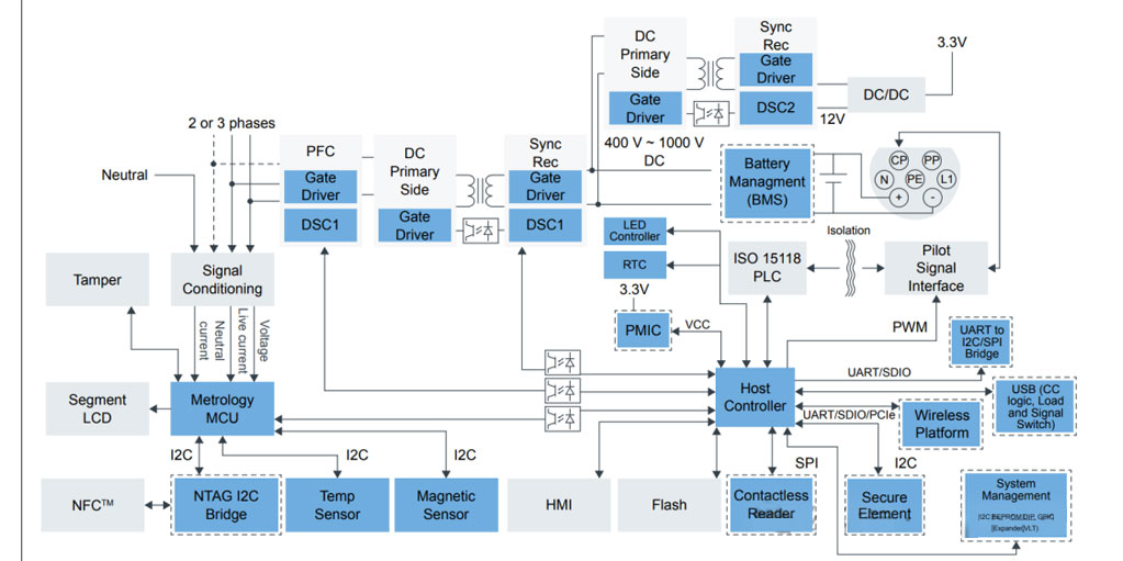
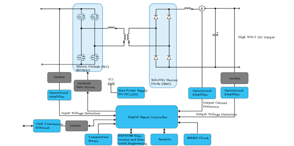
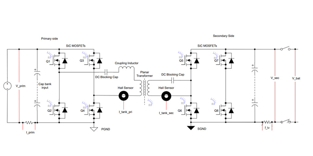
A Level 3 DC fast charger bypasses the EV's On-Board Charger (OBC) and charges the battery directly through the EV Battery Management System (BMS). Bypassing the OBC significantly boosts charging rates, with charger output power ranging from 50 to 350 kW. Common output voltages are 400–800V, while newer EVs tend to utilize 800V batteries. Since Level 3 (L3) DC fast chargers must convert three-phase Alternating Current (AC) input voltage to DC, they incorporate an AC-DC Power Factor Correction (PFC) frontend with an isolated DC-DC converter to connect the PFC output to the EV's battery. Multiple power modules are typically connected in parallel to achieve higher output power. The primary advantage of L3 DC fast chargers is their significant reduction in charging time.
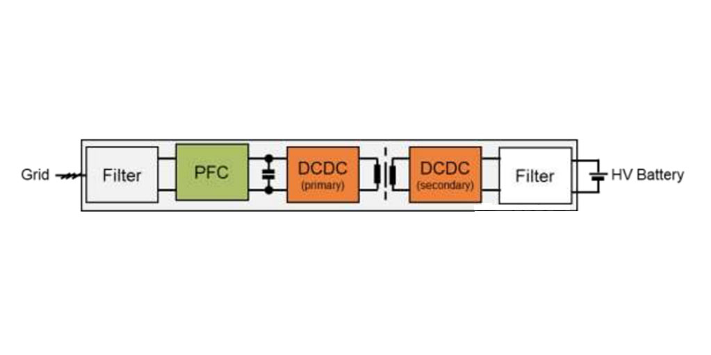
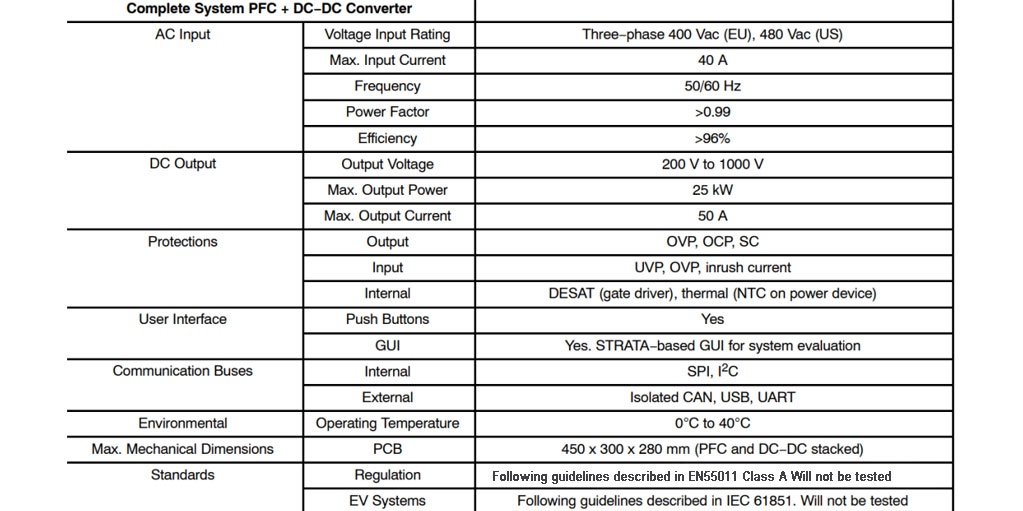
The core of a charging station is essentially a basic AC-DC converter. It comprises a PFC stage, a DC bus, and DC-DC modules.
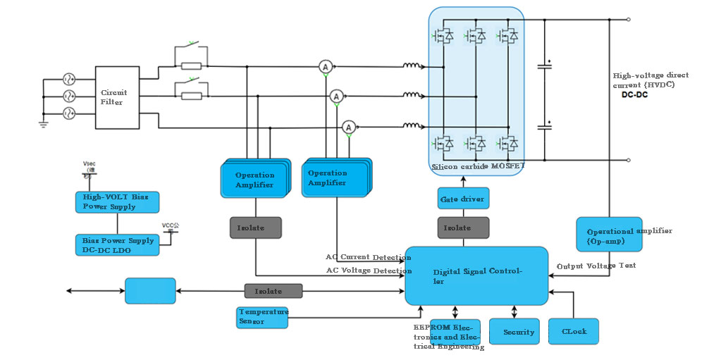
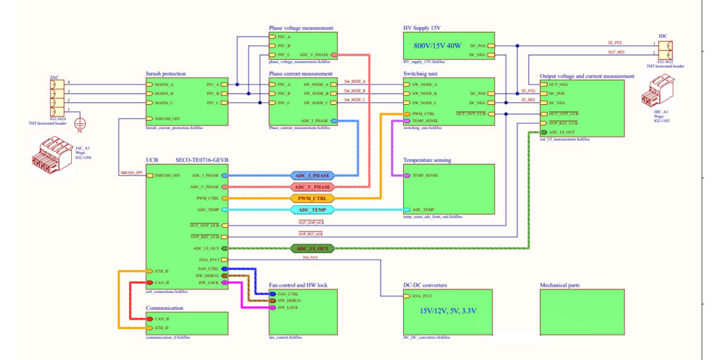
PFC Stage Functional Block Diagram
DC-DC Module Functional Block Diagram
Charging Station Scenario Solutions
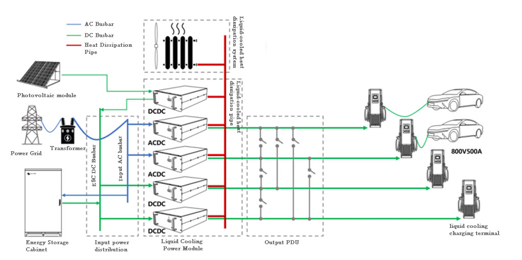
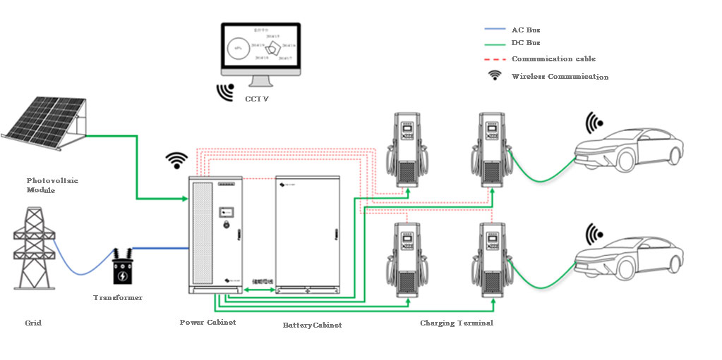
(1) Photovoltaic-Storage Charging System
Addressing the issue of increasing EV charging power and insufficient site distribution capacity, a storage charging system based on a DC bus is introduced. This system employs lithium-ion batteries as the energy storage device. Through local and remote Energy Management Systems (EMS), it balances and optimizes the supply and demand of electrical energy among the grid, batteries, and electric vehicles. It also facilitates integration with photovoltaic systems, offering benefits in peak-shaving, off-peak charging, and distribution network capacity expansion.
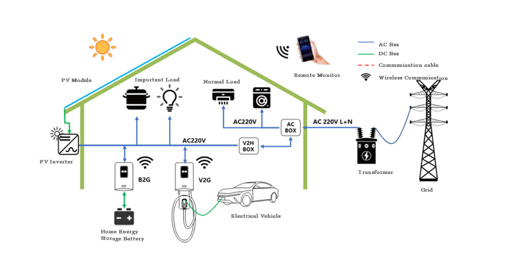
 (2) V2G Charging System
Vehicle-to-Grid (V2G) technology utilizes the energy stored in vehicle batteries to provide energy storage for the grid, enabling grid-vehicle interaction. This reduces the impact of large-scale renewable energy integration and mass EV charging on the grid's stability. Additionally, in residential communities and office parks, a unified EMS can manage a large number of EVs to achieve peak-shaving, dynamic capacity expansion, load-side response, and emergency power supply. For households, V2H (Vehicle-to-Home) devices can be used to leverage EV batteries for domestic energy storage.
(2) V2G Charging System
Vehicle-to-Grid (V2G) technology utilizes the energy stored in vehicle batteries to provide energy storage for the grid, enabling grid-vehicle interaction. This reduces the impact of large-scale renewable energy integration and mass EV charging on the grid's stability. Additionally, in residential communities and office parks, a unified EMS can manage a large number of EVs to achieve peak-shaving, dynamic capacity expansion, load-side response, and emergency power supply. For households, V2H (Vehicle-to-Home) devices can be used to leverage EV batteries for domestic energy storage.
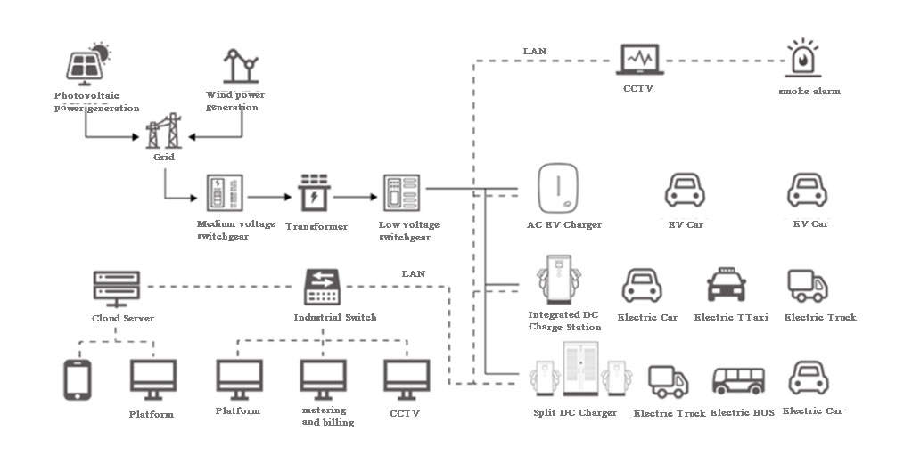
 (3) Ordered Charging System
This solution primarily utilizes high-power fast charging stations, ideal for centralized charging of urban buses, taxis, logistics fleets, etc. It allows for customized charging modes based on vehicle types. Vehicles can be charged during off-peak hours, reducing operational costs. An intelligent management system is provided for centralized vehicle management.
Future Development Trends
(1) Transition from Solely Centralized Charging Stations to a Diversified Scenario of Centralized + Distributed Complementary Development
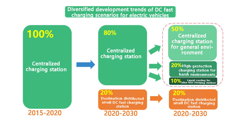
Destination-based distributed charging stations will serve as an effective supplement to the charging network. If traditional centralized charging stations are "people seeking charging piles," then destination-based distributed charging stations will be "piles waiting for people." Charging users can charge their vehicles while staying at their destinations (usually for over an hour), with less emphasis on charging speed timeliness (a certain level of top-up charging is sufficient). As a result, the charging power of these stations is primarily 20-30kW (mainly for passenger vehicles).
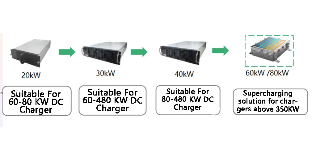
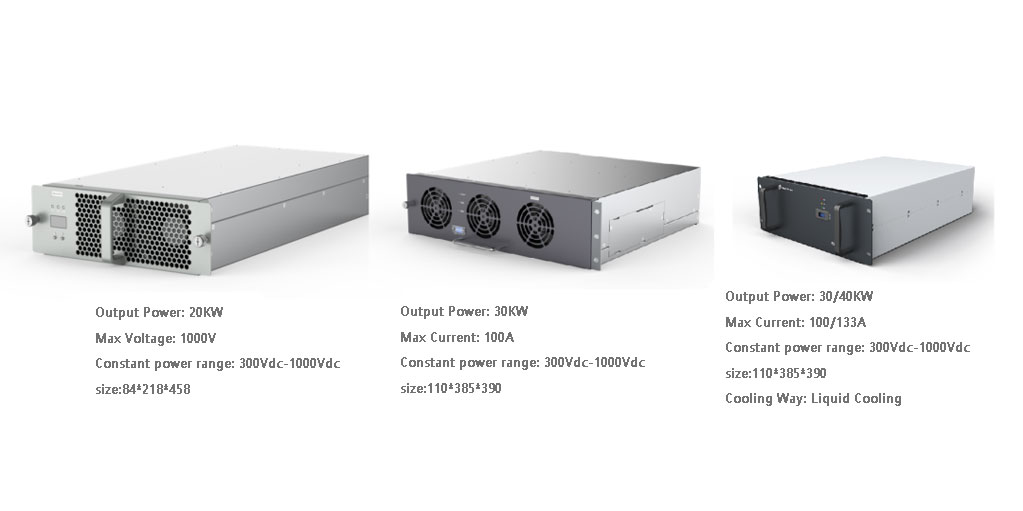
(2) Evolution from a Dominant 20kW Market Share to a Diversified Configuration Market of 20/30/40/60kW
The primary reason for this shift is that charging piles with different system powers and power distribution requirements for charging guns necessitate charging modules with varying optimal power granularities. Therefore, it is advisable to establish a series of charging modules with different capacities in terms of standard specifications.
(3) Expansion of Output Voltage Range Upper Limit from 750V to 1000V High Voltage
Under the trend of electrification towards higher voltages in electric vehicles, there is an urgent need for charging piles to increase their charging voltage upper limit to 1000V to support future high-voltage vehicle models. This will drive the upgrade of charging infrastructure. The highest output voltage of 1000V has become a consensus in the charging module industry, and major charging module manufacturers have gradually introduced 1000V high-voltage charging module specifications.
II. Introduction to Charging Pile Power Topology
PFC Rectifier Topology
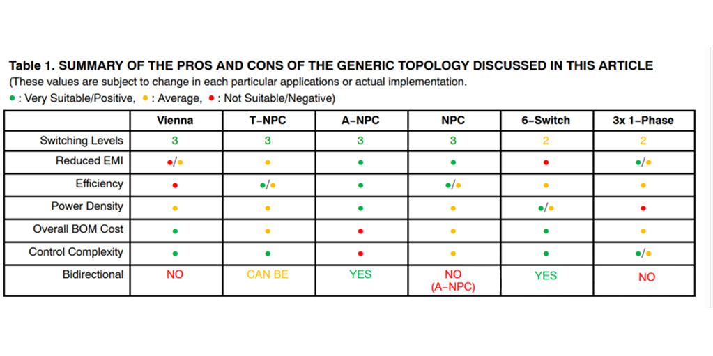
Topologies are classified into passive, hybrid, and active PFC rectifier systems. With recent advancements in semiconductor technology, active PFC is widely used in electric vehicle charging stations. Both single-phase and three-phase topologies are employed in EV charging stations, depending on the power level. Single-phase topologies are typically used for power levels below 3.3kW, while three-phase topologies are utilized for higher power levels. This section primarily introduces three-phase PFC topologies, namely, the conventional three-phase PFC topology, Vienna PFC, Neutral Point Clamped (NPC) 3-level PFC, and T-type NPC PFC.
(1) Three-phase PFC Topology
The typical configuration of a three-phase PFC is a six-switch boost rectifier with a very simple circuit topology and easy control characteristics. It facilitates bidirectional power flow and achieves a high power factor with reasonable efficiency. The working principle will be elaborated on later.
Since this topology is a two-stage design, it requires high-voltage blocking switches to withstand the entire DC link voltage. For instance, in an 800V DC link voltage application, the power stage necessitates silicon carbide (SiC) with a 1200V rated blocking capability. One drawback of this topology is the bulky filter inductor, which is necessary to regulate the input current THD to a lower value, resulting in low power density. Additionally, the peak voltage stress on the devices is very high, affecting the long-term reliability of semiconductors and other passive components used in the power stage. Compared to other popular multi-stage PFC topologies, the electromagnetic interference (EMI) performance of this converter is much lower.
(2) Vienna PFC Topology
The Vienna rectifier power topology is used in high-power three-phase power factor correction applications. Although there are numerous topologies for active three-phase power factor conversion, the Vienna rectifier remains popular due to its operation in continuous conduction mode (CCM), inherent three-level switching, and reduced voltage stress on power devices. Both hysteretic controllers and sine-triangle-based controllers are used for the Vienna rectifier, making control relatively simple as this topology requires less PWM. One drawback of this topology is that it only supports unidirectional power transfer from the grid to the DC side. The Vienna rectifier is characterized by a relatively small overall volume or high power density because it requires only about half the inductance of the boost inductor compared to a two-stage rectifier FPC. The multilevel feature of the output voltage also provides better THD performance. Unlike the three-phase PFC, the Vienna rectifier has a three-level characteristic, enabling high efficiency at higher switching frequencies with Si MOSFETs or 600V to 650V IGBTs and SiC Schottky diodes, without the need for advanced 1200V SiC power FETs to reduce switching losses.
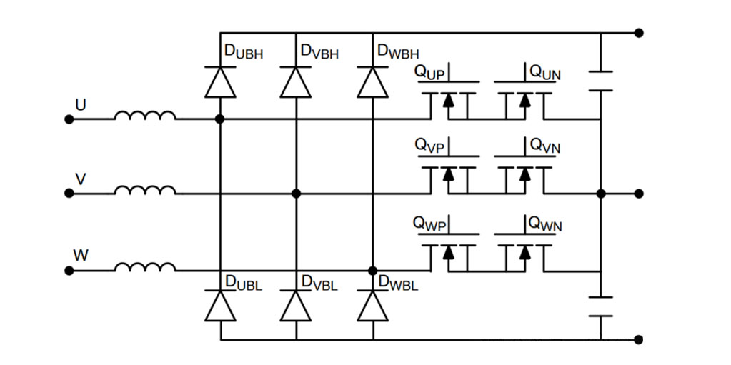
(3) Neutral Point Clamped (NPC) Topology
The basic topology of the Neutral Point Clamped (NPC) converter has been extended to three phases, where all switches in this topology only need to block half of the bus voltage. This results in the lowest voltage stress on devices among all topologies. Therefore, this topology can be easily scaled across multiple platforms using SiC, GaN, and Si MOSFETs, depending on the power level, cost, and target efficiency. Since only half of the voltage needs to be switched, this also reduces switching losses in MOSFETs by half, allowing the use of 600V components instead of 1200V types. Additionally, in 600V technology, the available speeds of components are much faster than in 1200V, further reducing switching losses. The NPC topology will have lower output current ripple and half the output voltage transients, reducing filtering and isolation work in the filter inductor. This enables high power density while reducing the inductance required to regulate the current waveform THD. Multilevel converters not only produce an output voltage with minimal interference but also minimize dv/dt stress on devices, thereby reducing electromagnetic interference (EMI) issues. Moreover, with lower switching losses and higher efficiency, this topology offers bidirectional power transfer and is the preferred choice for switching frequencies above 50kHz.
(4) T-type NPC Topology
The basic topology of the T-type converter extends the traditional two-level voltage source converter (VSC) topology with active bidirectional switches to the midpoint of the DC link. For an 800V DC link voltage, 1200V IGBTs/diodes are typically used on the high and low sides of each phase because they must block the full voltage. In contrast, the bidirectional switch at the midpoint of the DC link only needs to block half the voltage, which can be achieved with devices with lower voltage ratings, such as two 600V IGBTs with antiparallel diodes. Due to the reduced blocking voltage, the switching losses of the middle switch are ultra-low, and conduction losses are acceptable. For NPC topologies, direct transitions from the positive (P) level to the negative (N) DC link voltage level, and vice versa, are usually omitted because they can prevent uneven voltage sharing during transients when two series-connected FETs are turned off simultaneously. This adverse effect does not occur in the T-type topology. There is no need to implement low-level routines that prevent such transitions or ensure transient voltage balancing between series-connected IGBTs. An additional benefit of using a single 1200V device to block the full DC link voltage is reduced conduction losses. Whenever the output is connected to (P) or (N), only one device's forward voltage drop appears, in contrast to the NPC topology where two devices are always in series. Conduction losses are significantly reduced, making the T-type a good choice even at low switching frequencies.
(5) Conclusion
The T-type NPC topology boasts significantly lower conduction losses compared to the NPC, but suffers from high switching losses due to the blocking of the full DC link voltage by its devices. Despite the limited number of components, the T-type rectifier excels in efficiency, power density, and bidirectional operation capabilities compared to NPC topologies, as well as Vienna rectifiers and three-phase PFCs. Thus, it is ideally suited for applications with frequencies up to 50kHz (beyond which NPC performs better). One drawback of this topology is the high peak voltage stress on high-voltage blocking FETs. Nonetheless, similar to other topologies, it demonstrates excellent THD performance, eliminating the need for bulky inductors at the input end.
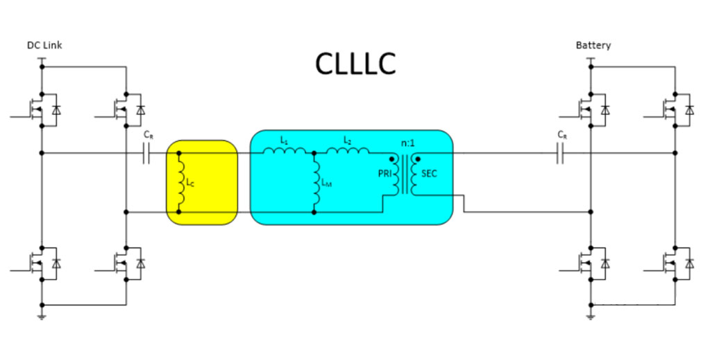
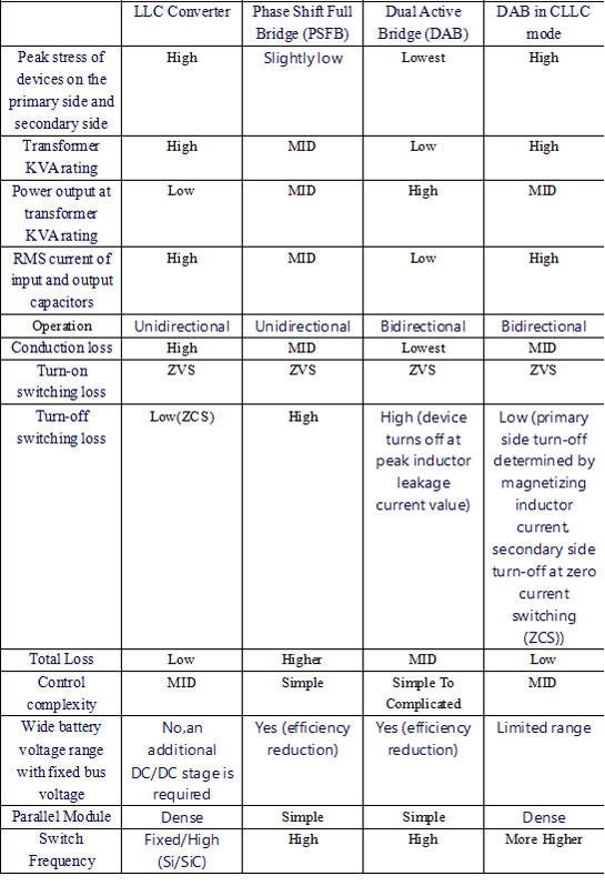
DC/DC Conversion Topologies
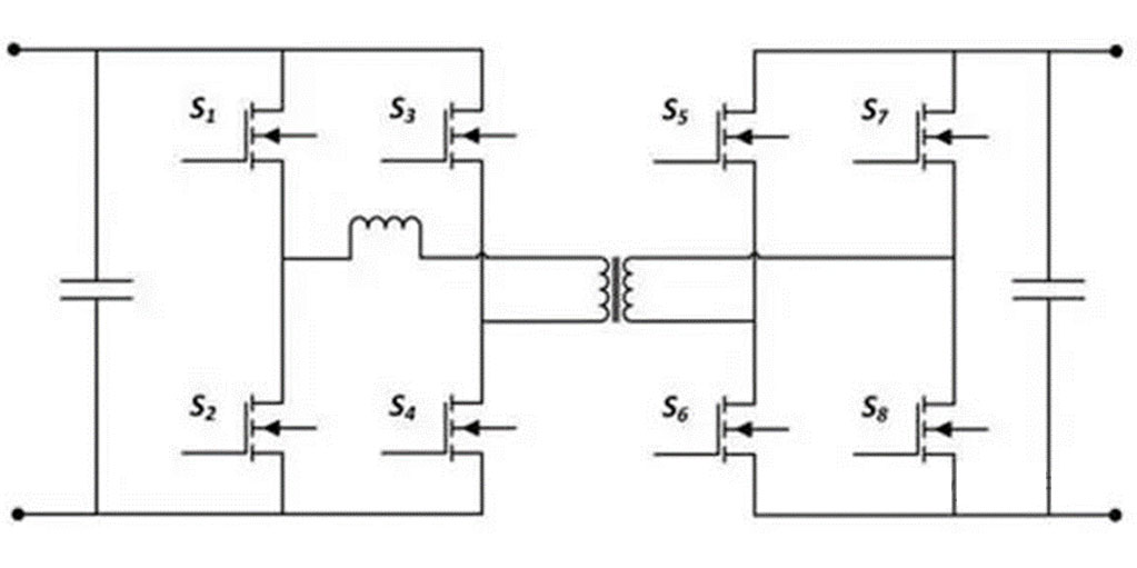
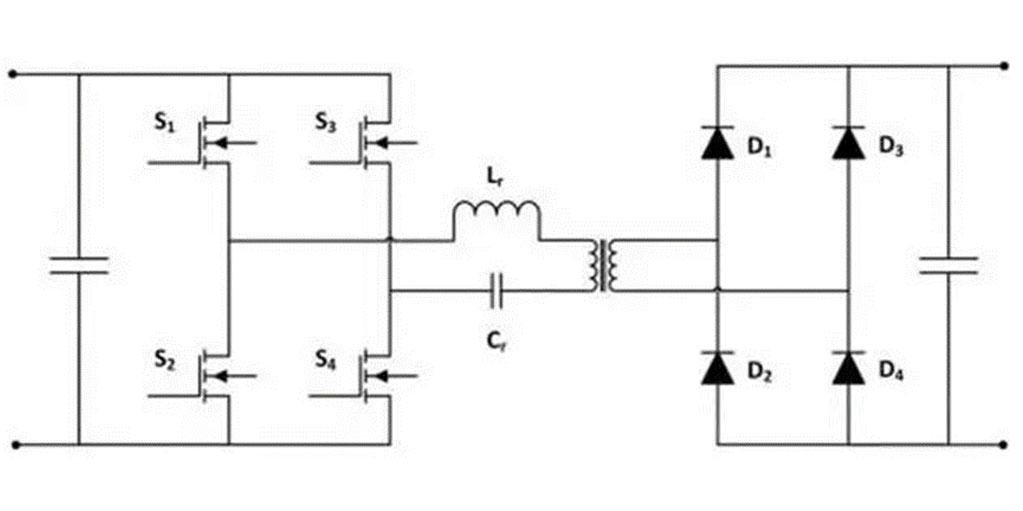
There are currently four mainstream high-power DC/DC converter topologies in the market: LLC resonant converters, phase-shifted full-bridge (PSFB), single-phase dual-active bridge (DAB), and dual-active bridge in CLLC mode (DAB – CLLC).
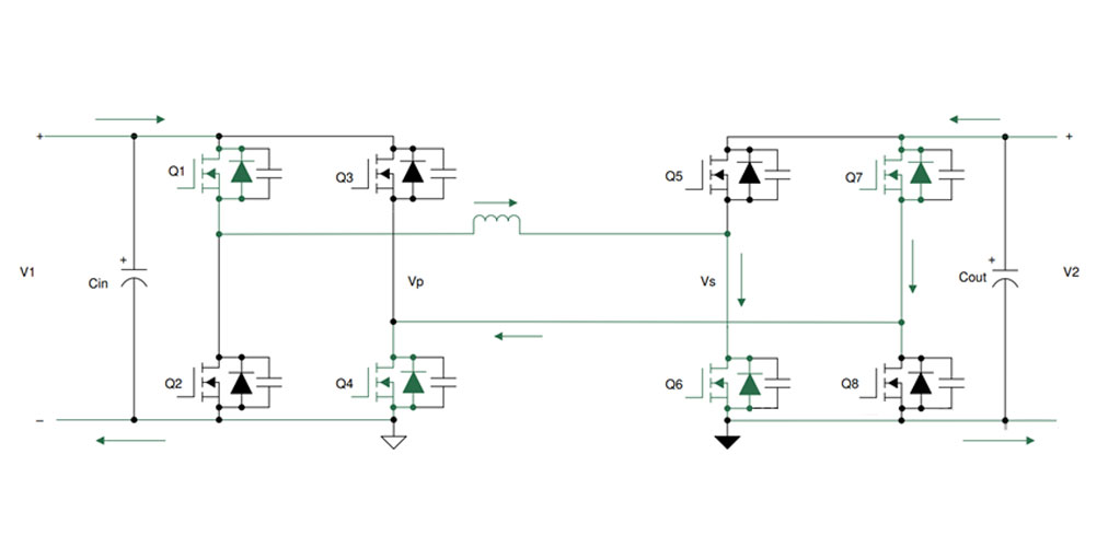
(1) Single-Phase Dual-Active Bridge (DAB)
The fundamental topology of the dual-active bridge converter comprises full bridges, with the active switches on the primary and secondary sides connected via a high-frequency transformer. Due to the inherent lagging current in one of the bridges, the current discharges the output capacitors of one bridge (e.g., secondary side) and certain switches on the primary side, enabling ZVS conduction. Furthermore, lossless capacitive snubbers can be employed on switches to reduce turn-off losses. The primary advantage of this converter lies in its inherent bidirectional functionality, achieved by controlling the phase angle between the two bridges, and its modularity allows for expansion to higher power levels. DAB control ranges from simple (or single-phase-shift modulation) to complex (extended, dual, and triple-phase-shift modulation). This topology can cover a wide range of battery voltage variations through single-phase-shift modulation, but the circulating current in the transformer increases, significantly reducing efficiency. However, with advanced modulation schemes like triple-phase-shift, the converter can theoretically achieve ZVS throughout its operating range. For this topology, transformer KVA ratings offer high output power utilization. Additionally, the output capacitance required to handle ripple currents is low. The converter boasts a relatively low component count, soft-switching commutation, low cost, and high efficiency, making it suitable for applications where power density, cost, weight, isolation, and reliability are critical factors. A limiting characteristic is that the converter typically requires an additional magnetizing inductor, essential for ZVS operation, which can add bulk and impact power density.
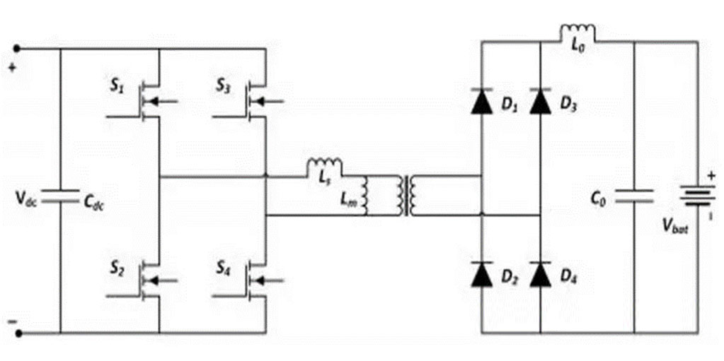
(2) LLC Resonant Converter
The gain of this converter is a function of the switching bridge gain, resonant circuit gain, and transformer turns ratio. Output voltage regulation is achieved by varying the operating switching frequency. LLC resonant converters operate in three modes/regions: below, at, and above the resonant frequency. Operating below the resonant frequency results in the resonant half-cycle inductor current reaching the magnetization current value within the switching cycle, enabling soft-switching between secondary rectifier diodes but increasing conduction losses due to increased circulating energy. Operating above the resonant frequency leads to increased switching losses and hard commutation of the secondary rectifier diodes but reduced conduction losses due to decreased circulating energy. Thus, these converters exhibit exceptional performance when operated close to the resonant frequency, enabling ZVS turn-on and ZCS turn-off. The converter provides unidirectional power flow and is commonly used in applications with power levels below 5kW. Paralleling and synchronizing multiple LLC converter modules to increase power throughput is challenging and often requires external control logic for safe implementation. Low di/dt in high output voltage designs (above 400V) complicates the implementation of synchronous rectification in LLC converters. Ripple currents and peak voltage stresses on active and passive devices are significantly higher, necessitating larger output capacitors to handle high ripple. Moreover, the transformers in LLC converters are slightly larger, significantly reducing the converter's power density. However, due to its soft-switching during turn-on and turn-off, the converter exhibits better EMI performance.
(3) Phase-Shift Full-Bridge (PSFB)
PSFB controls the power transfer between the primary and secondary sides by altering the phase between the switching legs of the primary bridge. Consequently, one leg achieves Zero-Voltage Switching (ZVS) conduction, while the other leg facilitates low-voltage conduction, significantly reducing losses. The passive diodes on the secondary side may experience hard switching, leading to increased conduction losses and thus reducing the converter's efficiency. Under light-load conditions, the converter encounters non-ZVS conduction losses during turn-on and turn-off. Typically, burst-mode operation is employed to maintain ZVS under light loads. This converter is also modular, allowing parallel connection for higher power throughput in electric vehicle charging stations. In PSFB, jitter can be readily implemented to mitigate conducted Electromagnetic Interference (EMI) signals. This topology necessitates a DC-blocking capacitor to prevent transformer saturation due to DC voltage offsets in voltage-mode control. Additionally, the converter often requires an extra resonant inductor, essential for ZVS operation, which can make the converter bulky and impact power density.
(4) CLLC Topology
The CLLC incorporates all the functionalities of the LLC mentioned earlier, but its primary advantage lies in enabling bidirectional power transfer through the use of active switches on the secondary side. The converter's ZVS/Zero-Current Switching (ZCS) operation enhances efficiency. When the bus voltage has a 10% margin variation, this converter can accommodate wide-ranging battery voltages with excellent efficiency performance. However, with a fixed bus voltage, its operating range is quite limited. The use of capacitors on both the primary and secondary sides of the transformer prevents transformer core saturation issues. This converter is primarily suited for onboard charger applications but can be utilized at higher power levels up to 10kW. However, scaling to higher power levels and paralleling can be challenging due to the need for highly symmetric capacitor structures and synchronization across multiple modules, which can be complex.
(5) Conclusion
III. Introduction to PFC+DAB Principles
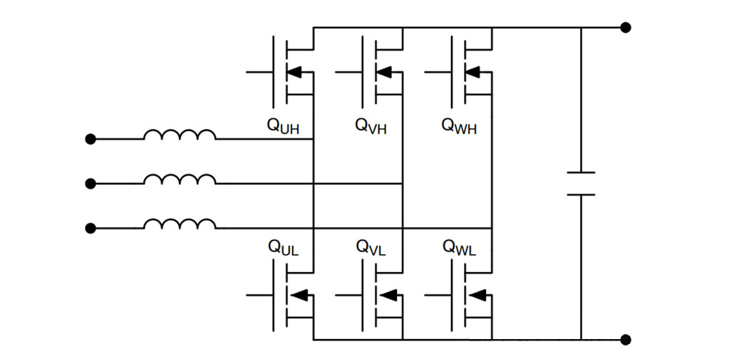
PFC Working Principle
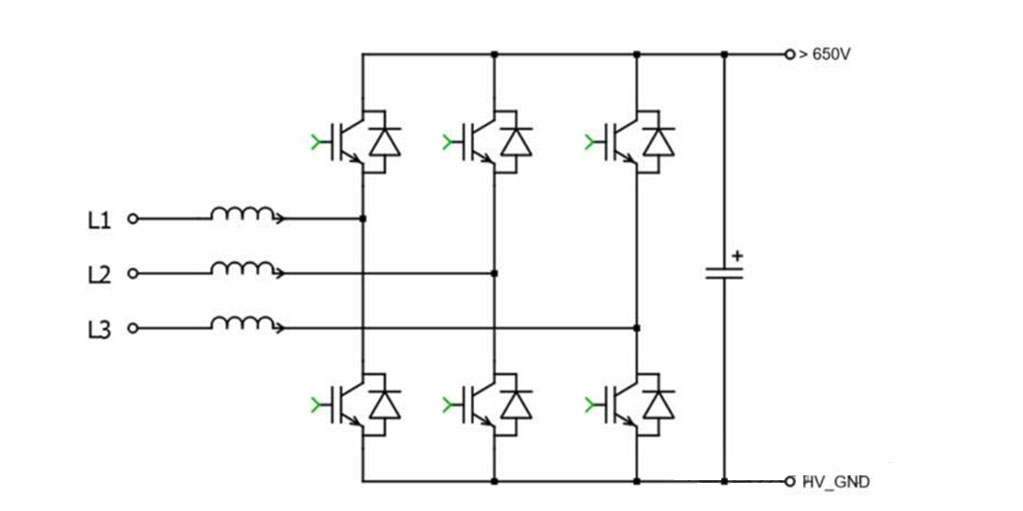
A well-established topology for a three-phase AC grid is the three-phase full-bridge PFC, also known as B6 or "three-leg bridge." This topology operates solely with three-phase AC inputs. For single-phase operation, a neutral line can be added easily. A three-phase power source comprises three AC phases, typically denoted as L1, L2, and L3. These phases generate sinusoidal voltages with equal amplitudes and frequencies (referenced to ground potential), with their phases shifted by 120° from each other.
The phase sequence of a three-phase power source can be monitored by measuring the phase shifts (in time) between the three sinusoidal signals. In positive phase sequence, the voltages on all three lines of the three-phase source complete a 360° cycle, with L2 lagging L1 by 120°, and L3 lagging L1 by +240°. The sequence L1 – L2 – L3 is referred to as positive phase sequence.
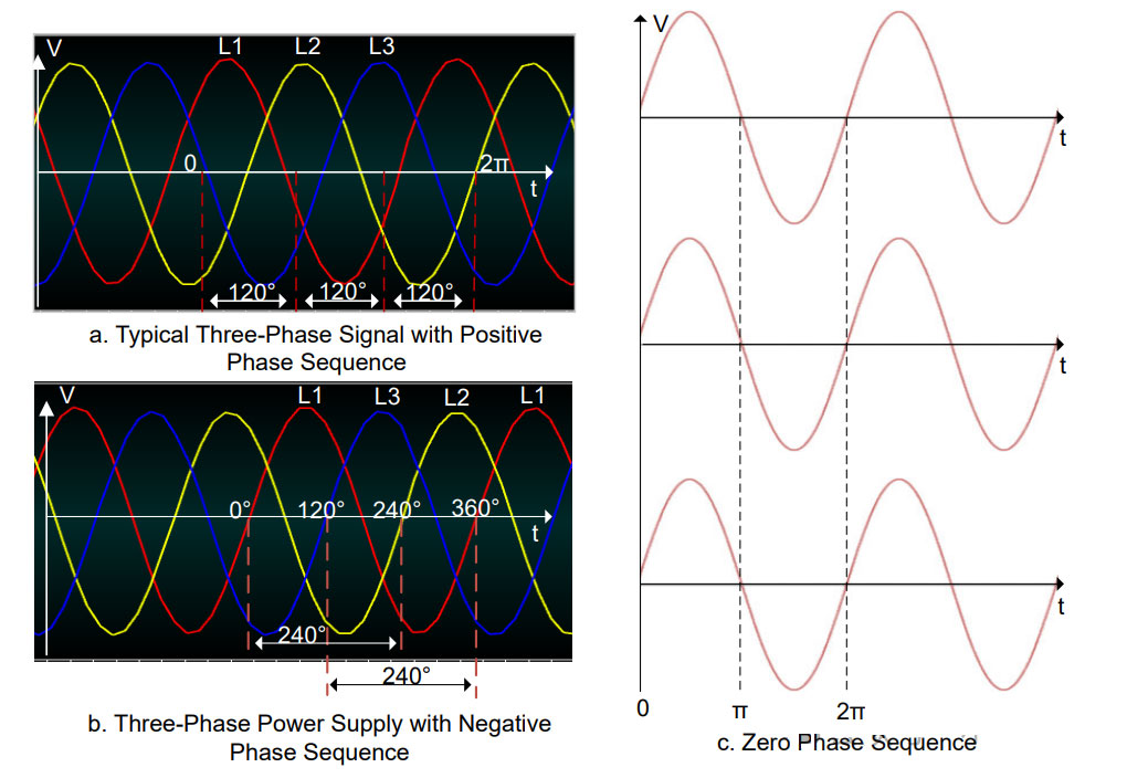
In negative or reverse phase sequence, the voltages on all three lines of the three-phase source also complete a 360° cycle, but with L3 lagging L1 by 120° and L2 lagging L1 by +240°. The sequence L1 – L3 – L2 is known as negative or reverse phase sequence.
When L1, L2, and L3 phases are in parallel, it is termed zero phase sequence.
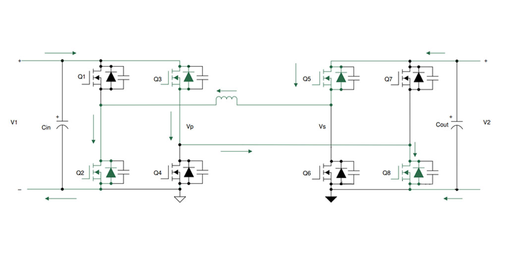
2. Working Principle of Dual Active Bridge (DAB)
The power transfer between two bridges in a Dual Active Bridge (DAB) resembles the power flow between two voltage buses in a power supply system.
During power transfer in a DAB, two high-frequency square waves are generated on the primary and secondary sides of the transformer through MOSFET switching operations. These two high-frequency square waves exhibit a phase shift relative to each other. Power is transmitted from the leading bridge to the lagging bridge, and the direction of this power flow can be easily reversed by inverting the phase shift between the two bridges. Consequently, bidirectional power transfer can be effortlessly achieved in a DAB.
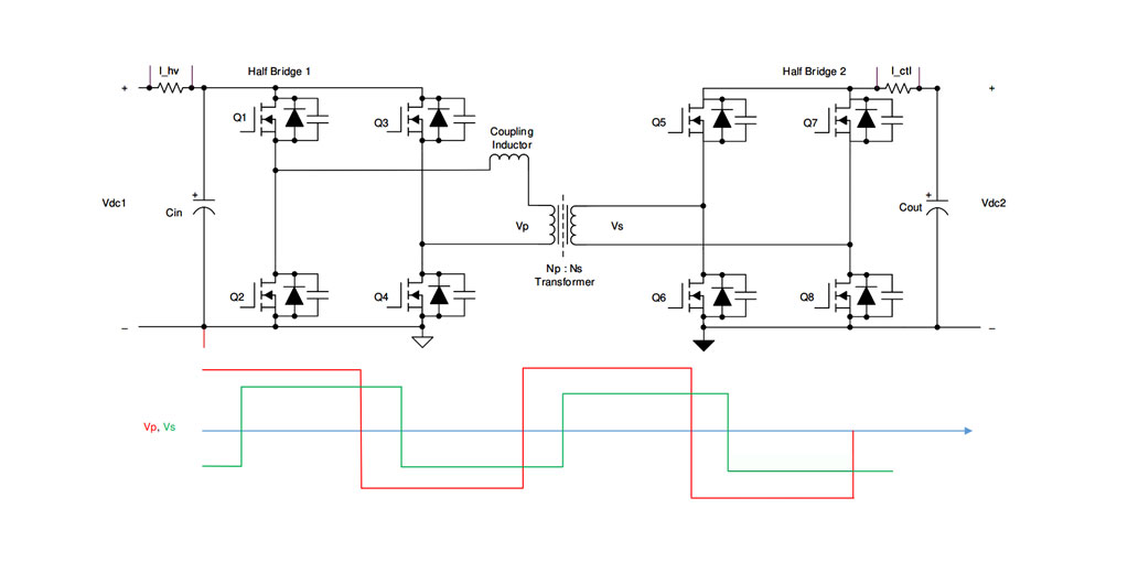
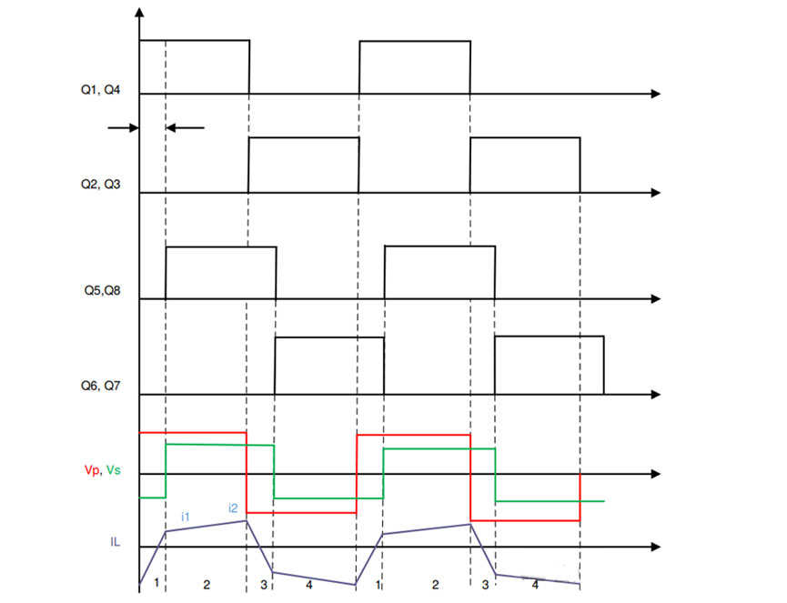
(1) Switching Sequences
In a single-phase DAB, both the primary and secondary bridges are controlled simultaneously. All switches operate with a 50% duty cycle. Diagonal switches turn on and off together, resulting in square wave outputs from each bridge. Depending on the inductor current waveform and the phase shift between the primary and secondary voltages of the transformer, the switching sequences are divided into four phases:
Phase 1
The voltage Vp on the primary side equals V1, while the voltage Vs on the secondary side equals V2. The difference between these two voltages appears across the leakage inductor, and the current slope during this interval is:
dt/di=(V1+V2)/L
Phase 2
The inductor current is positive. The voltage on the primary side of the transformer is positive, equal to V1, and the voltage on the secondary winding is also positive, equal to V2. Therefore, the difference between these two voltages appears across the leakage inductor, and the slope of the rising current during this interval is:
dt/di=-(V1-V2)/L
Phase 3
The inductor current begins to decrease from its positive peak to a negative value. During this interval, the voltage on the primary side is –V1, while the voltage on the secondary side is V2. The difference between these two voltages (i.e., (-V1-V2)) appears across the inductor, causing the current to decrease with a negative slope:
dt/di=-(V1+V2)/L
Phase 4
The inductor current remains negative. During this interval, the voltage on the primary side is –V1, and the voltage on the secondary side is -V2. The difference between these two voltages (i.e., (-V1+V2)) appears across the inductor, causing the current to continue decreasing with a negative slope:
dt/di=(V1-V2)/L
Waveform Diagram
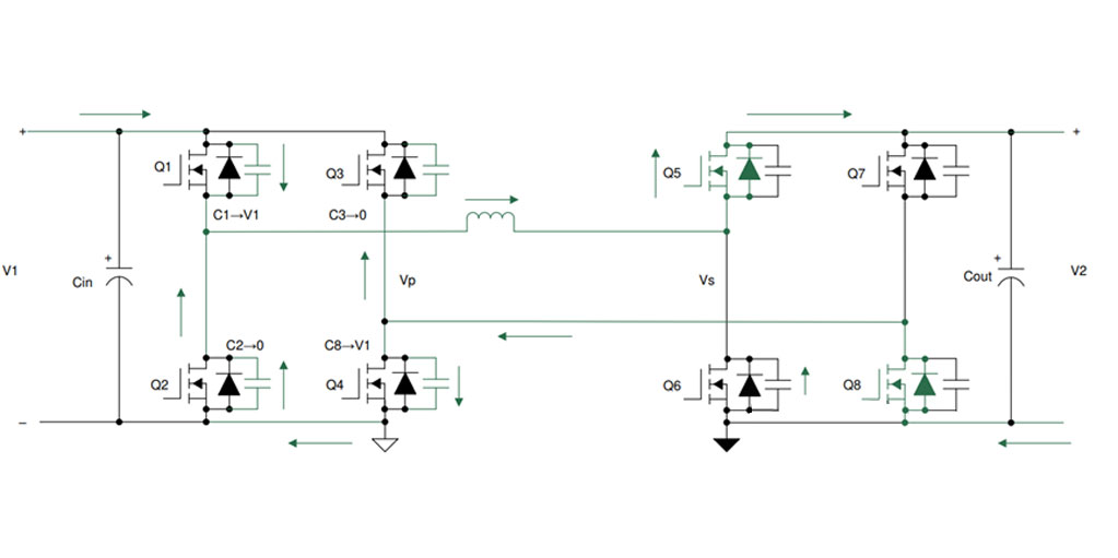
(2) Zero-Voltage Switching (ZVS)
There exists a dead time between the turn-off of one MOSFET and the turn-on of another in a leg. During this dead time, the energy stored in the inductor discharges the output capacitors of the MOSFETs, bringing their voltages close to zero before conduction. This phenomenon, where the voltage across a MOSFET approaches zero during turn-on, is known as Zero-Voltage Switching (ZVS).
Due to the natural lagging current in one of the bridges, the energy stored in the inductor causes ZVS in all switches of the lagging bridge and some switches of the leading bridge. This depends on the stored inductor energy (EL = 0.5LI²), which is used to charge and discharge the output capacitors of the MOSFETs (EC = 0.5CV²), and also on the converter's load and input-output voltage ratio.
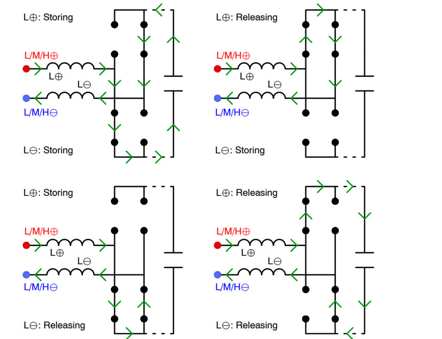
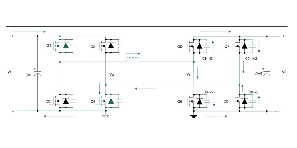
ZVS Switching on the Secondary Side - Capacitors
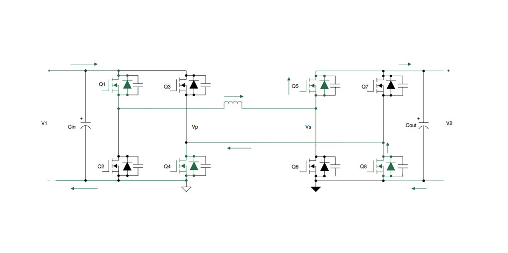
Primary-side switches Q1 and Q5 remain on, while secondary-side switches Q6 and Q7 turn off, and switches Q5 and Q8 turn on. Initially, when Q6 and Q7 are on, their voltages are zero, while Q5 and Q8 block the entire secondary voltage. During the dead time, when all secondary-side switches are off, the energy stored in the inductor circulates the current, discharging the capacitors on MOSFETs Q5 and Q8 to zero and charging the capacitors on MOSFETs Q6 and Q7 to full.
ZVS Switching on the Secondary Side - Diodes
Once the capacitors are charged and discharged, the current must continue to flow. It flows through diodes D5 and D8, clamping the voltages on MOSFETs Q5 and Q8 to zero. During the next interval, MOSFETs Q5 and Q8 turn on under zero-voltage conditions, significantly reducing
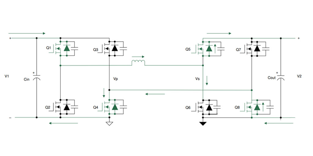
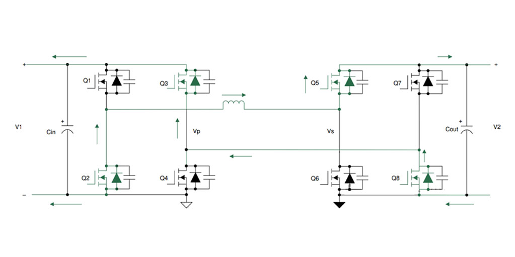
ZVS Switching on the Secondary Side - Diodes
Once the capacitors are charged and discharged, the current must continue to flow. The current will then pass through diodes D2 and D3, clamping the voltage across MOSFETs Q2 and Q3 to zero. During the subsequent interval, MOSFETs Q2 and Q3 conduct under zero-voltage conditions, thereby significantly reducing conduction losses. The arrows next to the diodes indicate that the diodes are conducting, while the MOSFETs are off.
Output Waveform Diagrams
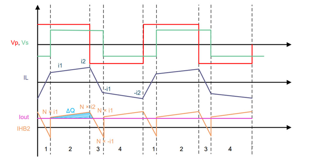
Diagram: Current through the Output Capacitor
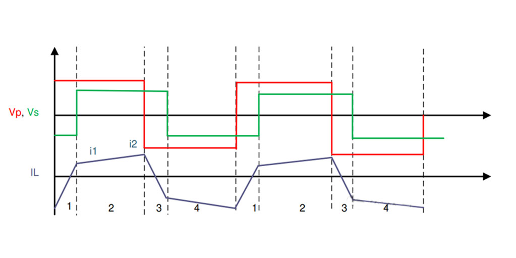
Diagram: Inductor Current Waveform
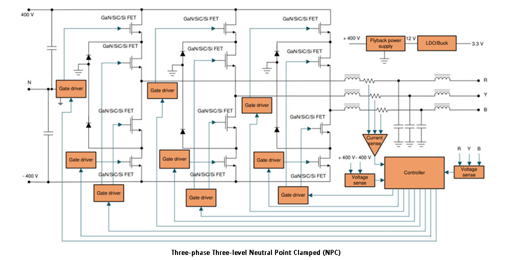
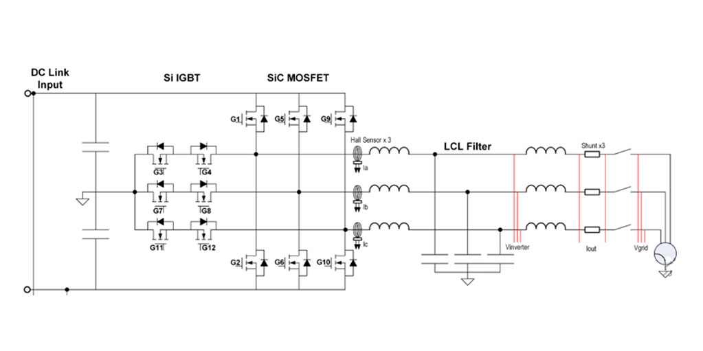
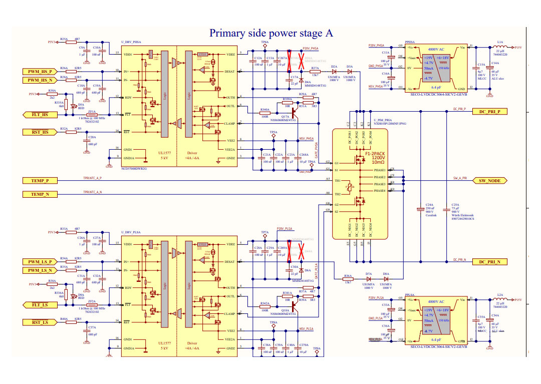
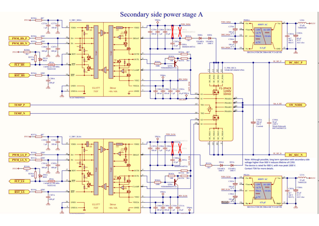
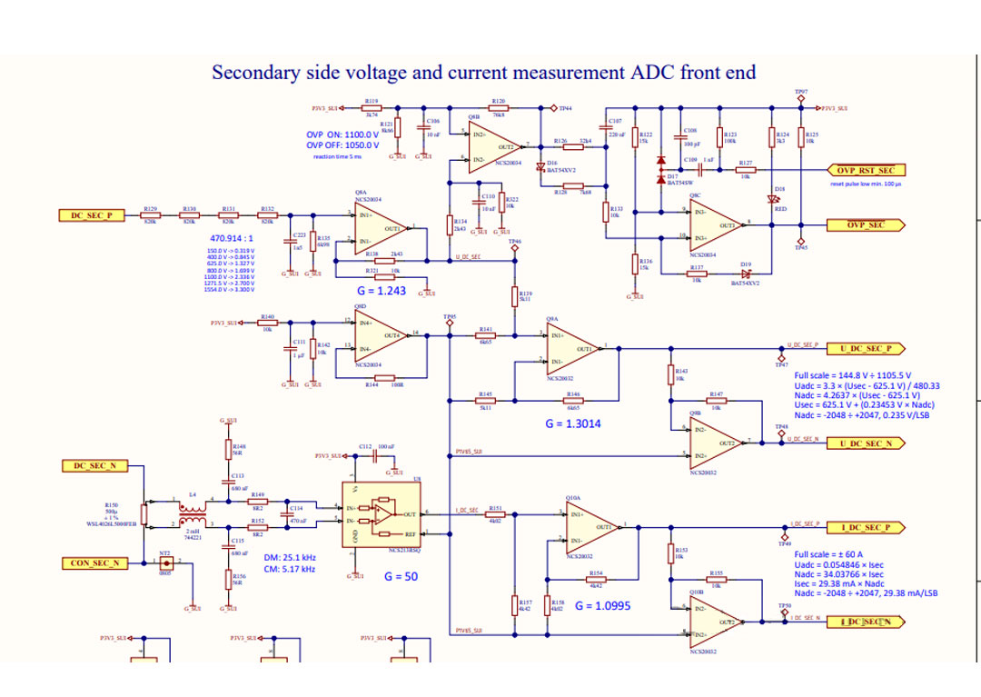
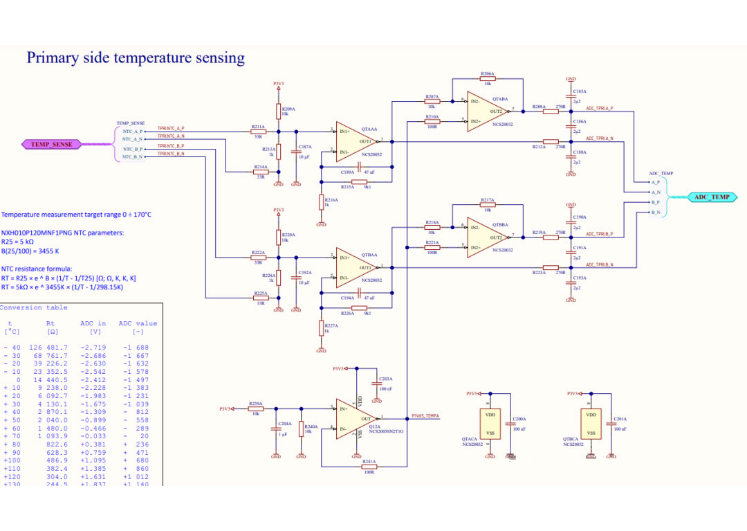
IV. Introduction to the Charging Station Module Scheme
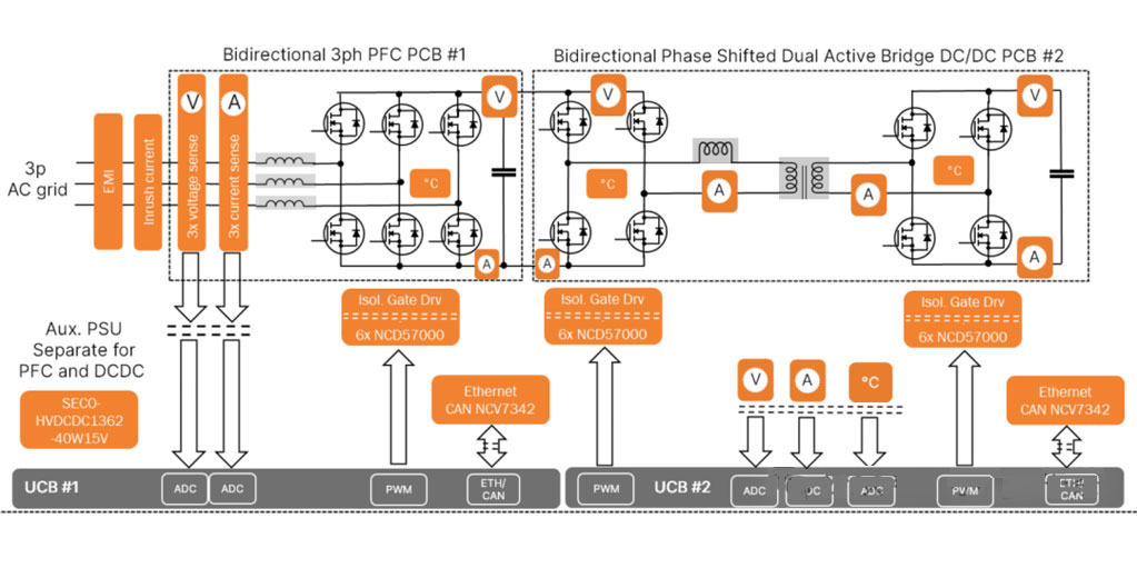
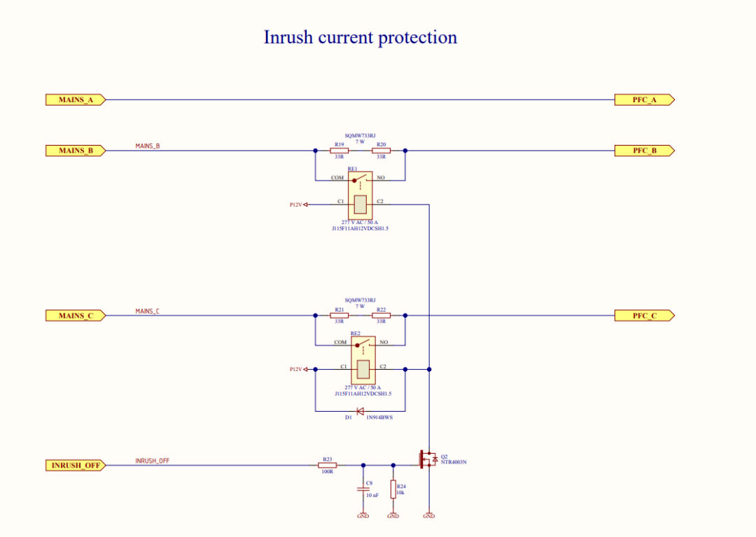
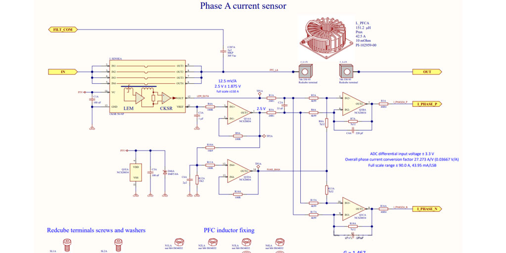
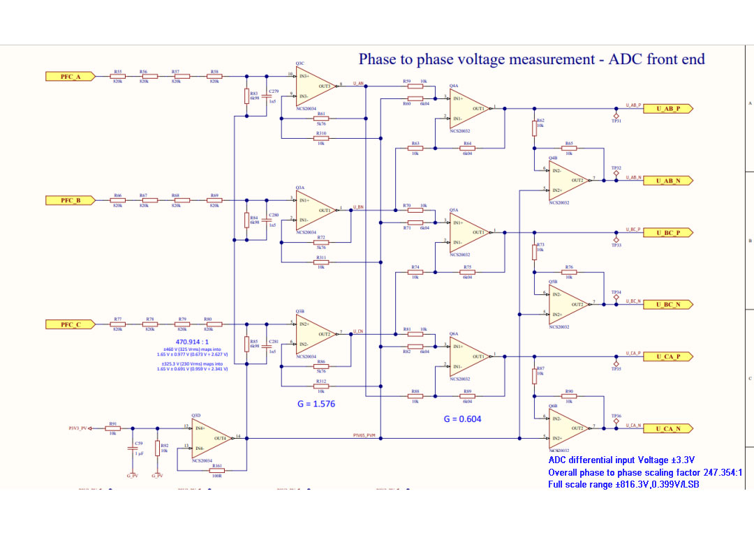
PFC Schematic Diagram
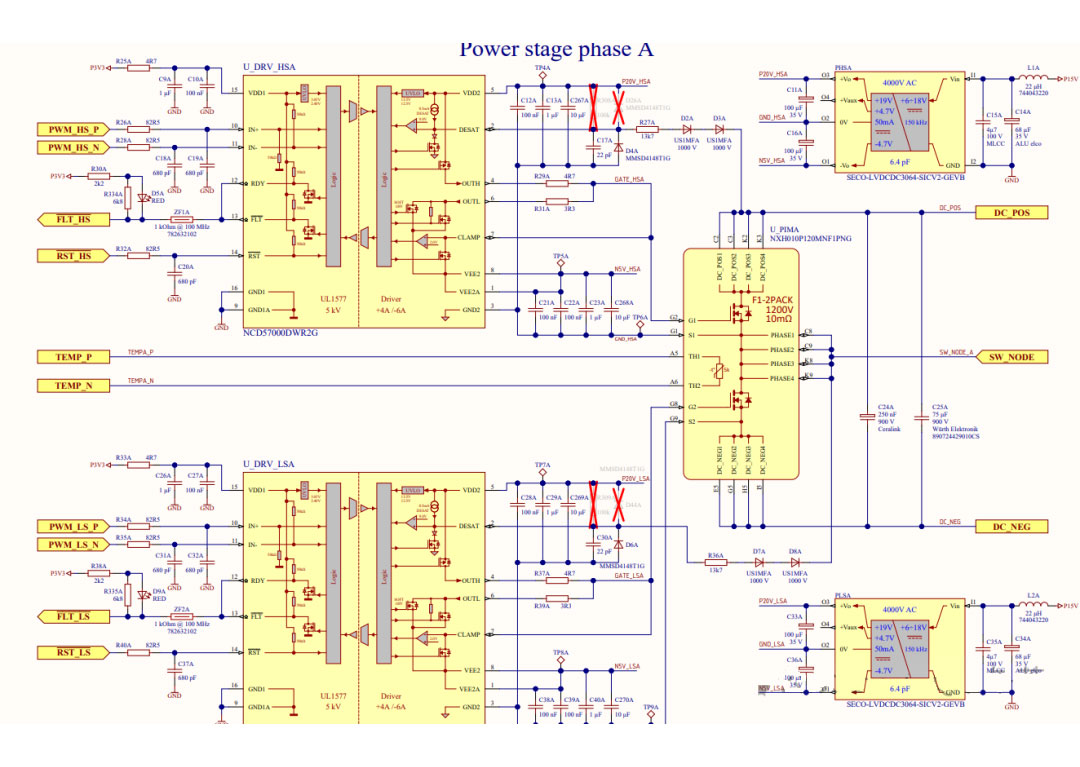
DAB Schematic Diagram
 English